新着情報

ASICON
published on
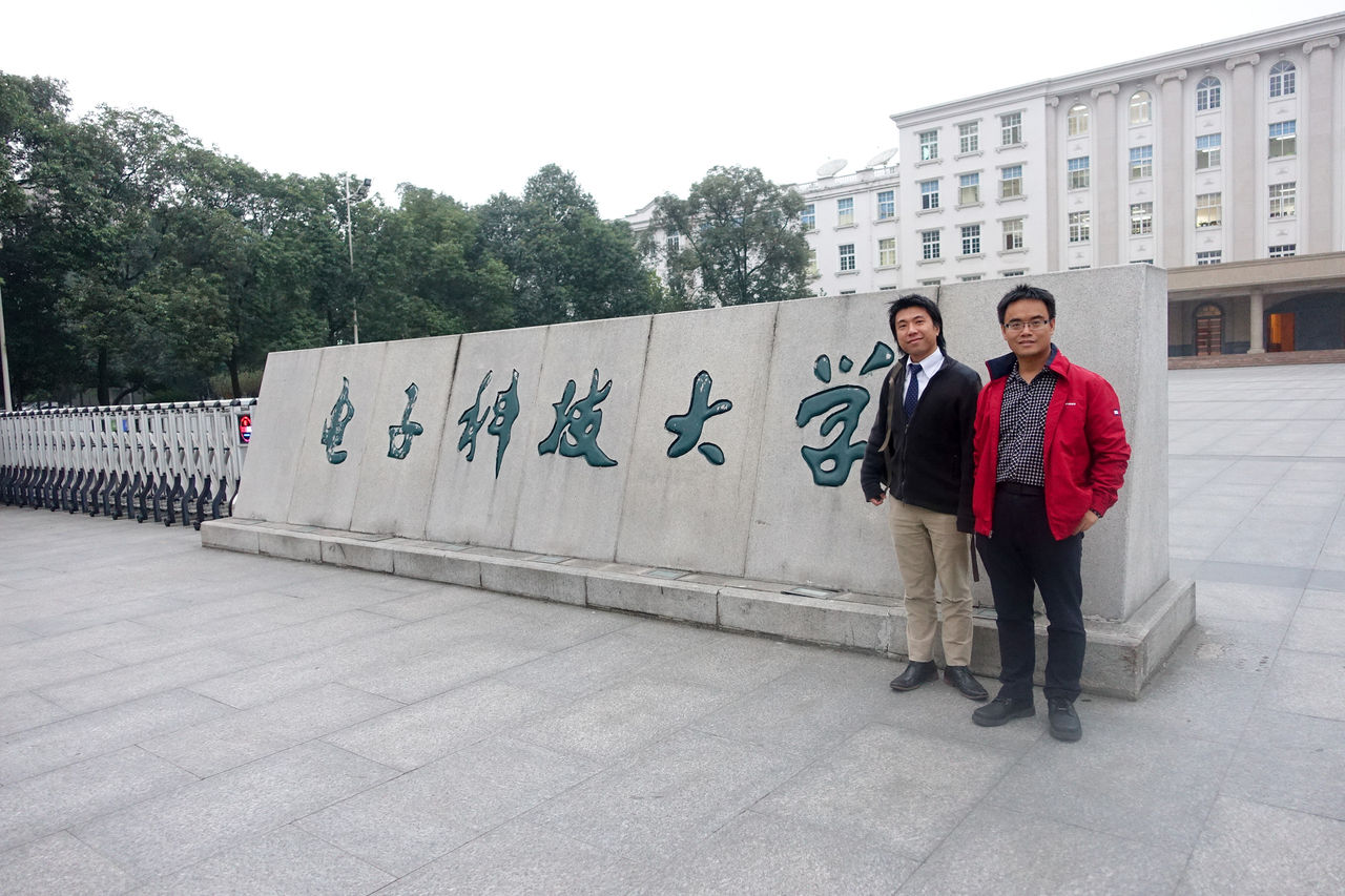
UESTC
電子科技大学(UESTC)のProf. Kai Kang先生を訪問しました。
エレクトロニクス実装学会 講演大会@東工大 3/22-24
エレクトロニクス実装学会の講演大会@東工大の締め切りは 11/25 です。是非とも投稿ください!
==============================================================第30回エレクトロニクス実装学会春季講演大会 発表申込み募集のお知らせ 2016年3月22日-24日 東京工業大学 大岡山キャンパス 詳しくは以下のリンクを参照ください。 http://e-jisso.jp/event/taikai/030.html==============================================================
1.開催概要> 1)日時:
>
> 2016年3月22日(火)から24日(木)
>
>
>
>
> 2)場所:
>
> 東京工業大学 大岡山キャンパス:西9号館(講演セッション、ポスターセッション、ものづくりセッション)
>
> 東工大蔵前会館くらまえホール(予定)(表彰式、特別講演、交流会)
>
> 地図 http://www.titech.ac.jp/maps/index.html
2.講演セッション> 「講演セッション」は、最新の実装技術分野の研究成果を発表し、議論するセッションです。
>
>
>
>
> 2)予稿:
>
> 論文形式でA4サイズ1~4頁
>
>
>
>
> 3)講演:
>
> 15分(発表時間12分、討論時間3分)
>
>
>
>
> 4)講演内容:
>
> 最近行った研究および調査の報告、または成果をあげた試験結果や技術開発の報告等で、学術的・工業的に価値のある未発表のものに限ります。ただし、内容が不適当(商品宣伝色濃厚、他者非難に終始したもの、等)であるものは採択されません。ICEPに投稿予定の研究開発成果について、その概要などを発表することができます。また、講演内容を含めて「エレクトロニクス実装学会誌」に投稿することもできます。
>
>
>
>
> 5)表彰:
>
> 優れた論文発表に対し、講演大会優秀賞(表彰対象者は共著者を含む全員)、同賞以外の優秀な発表をした若手発表者(発表時、満35歳未満)に研究奨励賞を授与します。
>
>
>
>
> 6)募集テーマ:
>
> 発表論文の募集分野は以下の19テーマです。
>
> (1)カーエレクトロニクス:
>
> (2)ヘルスケア:
>
> (3)サーマルマネージメント&パワーエレクトロニクス:
>
> (4)部品内蔵基板:
>
> (5)プリンタブルデバイス実装:
>
> (6)三次元造形配線・実装応用技術
>
> (7)官能検査システム化技術
>
> (8)材料技術:
>
> (9)高速伝送実装:
>
> (10)回路・実装設計技術:
>
> (11)高速高周波・電磁特性技術:
>
> (12)配線板とその製造技術:
>
> (13)信頼性解析技術:
>
> (14)電子部品・実装技術:
>
> (15)検査技術:
>
> (16)光回路実装技術:
>
> (17)環境調和型実装技術:
>
> (18)システムインテグレーション実装技術:
>
> (19)マイクロメカトロニクス実装技術:
3.ポスターセッション> 2)予稿:
>
> 論文形式でA4サイズ1~4頁(講演セッションと同じ)
>
>
>
>
> 3)ポスター展示
>
> (A0縦サイズ1枚):
>
> 開催期間中
>
>
>
>
> 5)表彰:
>
> 優れたポスター発表に対し、ポスターアワード(表彰対象者は共著者を含む全員)、同賞以外の優秀な発表をした若手発表者(発表時、満35歳未満)に研究奨励賞を授与します。 4.ものづくりセッション> 「ものづくりセッション」は、製品技術の紹介を目的としたセッションです。製品に使われている技術、開発にいたるまでに課題解決をした経験などを紹介するセッションです。
>
>
>
>
> 2) 予稿:
>
> 論文形式(講演セッションと同じA4サイズ1~4頁)または、スライド形式。(24枚以内、データサイズ8MB以内) スライド形式の場合、A4サイズ1ページ当たり6スライドでpdfファイル1~4頁を作成し提出ください。
>
>
>
>
> 3) 講演:
>
> プレゼンテーション(発表時間15分、質疑応答時間5分)
>
>
>
>
> 4) 展示コーナー
>
> 説明:
>
> ポスター展示(最大A0縦サイズ1枚)と説明(ポスター展示用パネルと小テーブル(90cm×45㎝程度)を用意します)また、必要により、ノートPC用程度の電源設備は用意します。(展示コーナーのみの発表は受付けません。)
>
>
>
>
> 5) 広告掲載:
>
> プログラム冊子及び論文集CDに広告(A4サイズ1ページ)を掲載できます。
>
>
>
>
> 6) 募集分野:
>
> 発表分野は,以下の通りです。
>
> (1)設計技術
>
> (2)基板・実装材料
>
> (3)プロセス技術(回路形成技術、めっき技術、ビア形成技術等)
>
> (4)バンピング・アセンブリ技術
>
> (5)検査・試験・信頼性評価技術
>
> (6)各種製造装置(回路形成、アセンブリ、検査等)
>
> (7)電子部品(能動素子、受動素子、表示デバイス、電池等)
>
> (8)実装製品(小型・薄型実装機器、各種モジュール等)
>
> (9)その他
5.発表申込み学会webの「発表申込み」ページへお進みください。 http://e-jisso.jp/event/taikai/030.html★前回に続き、「発表申込み」と「参加登録」を分離し、発表者も改めて「参加登録」を行う手順になりました。「発表申込み」をされた方も、後日改めて「参加登録」をお願いします。① **発表申込み締め切り:2015年11月25日(水)(アブストラクト50-300文字含む)**③ 予稿原稿提出締切:2016年1月29日(金)

バレンタイン17年
published on
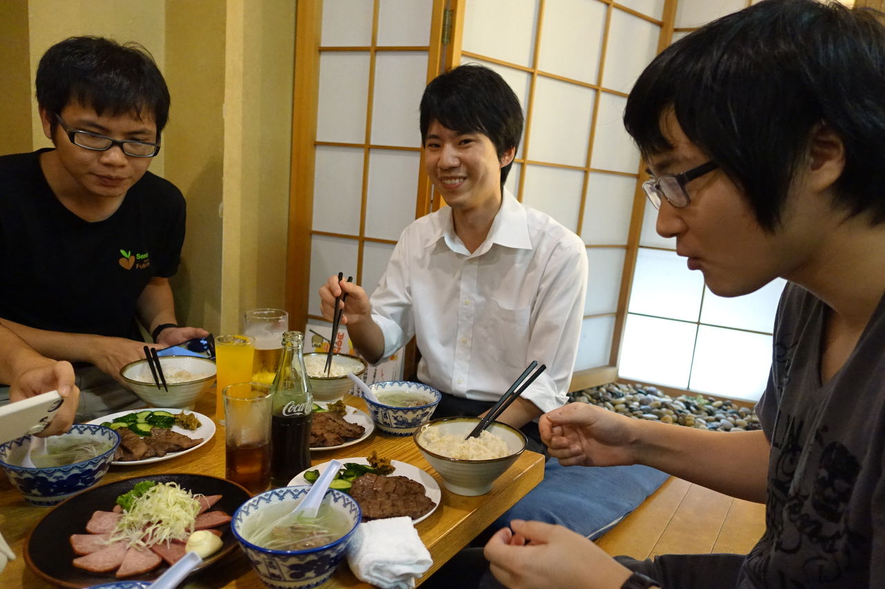
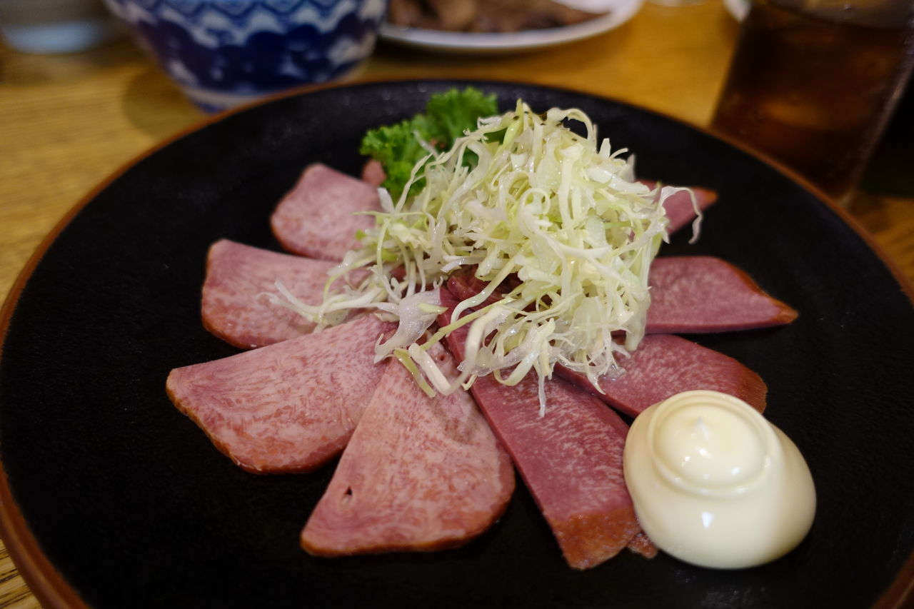
肉
published on
welcome party
published on
Apple
ISSCCのTPC meetingの後、CupertinoのApple本社を訪問し、本研究室OBのDr. Wei Deng氏と会談を行いました(岡田)。研究生活をEnjoyしているそうです!

Prof. Mehmet Unlu
published on
M2就活お疲れ飲み
published on
投稿お疲れ様でした!
published on
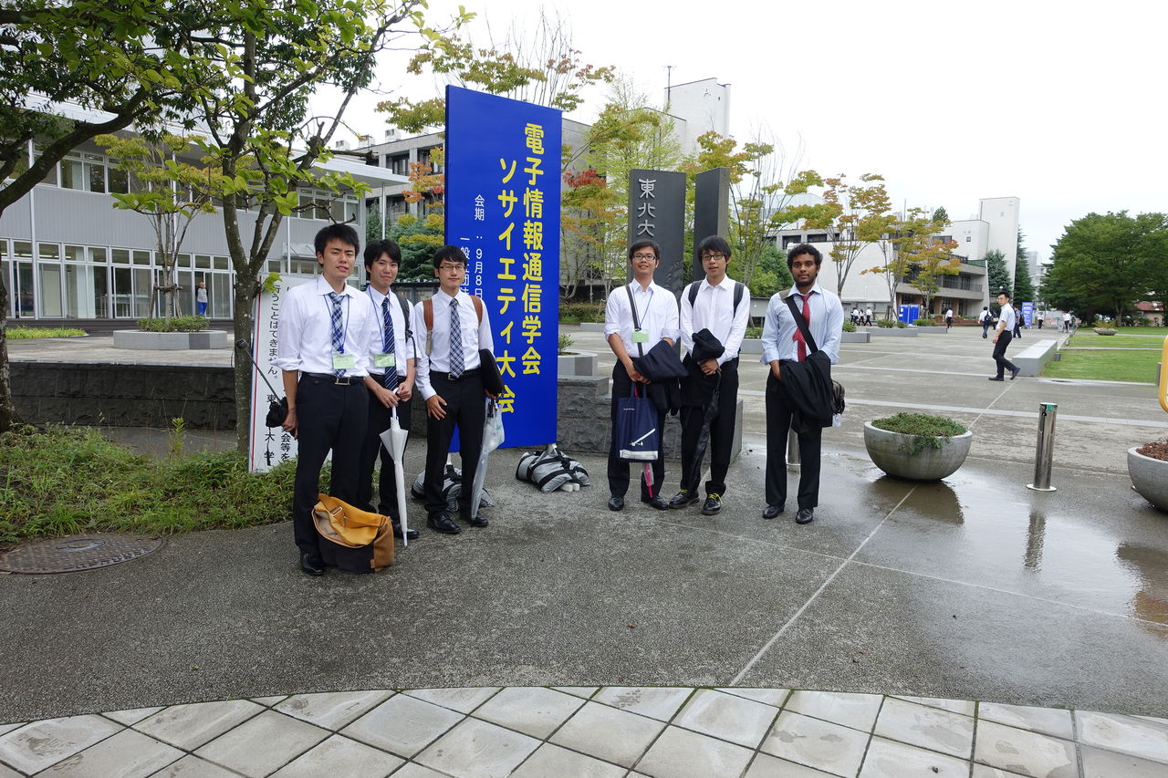
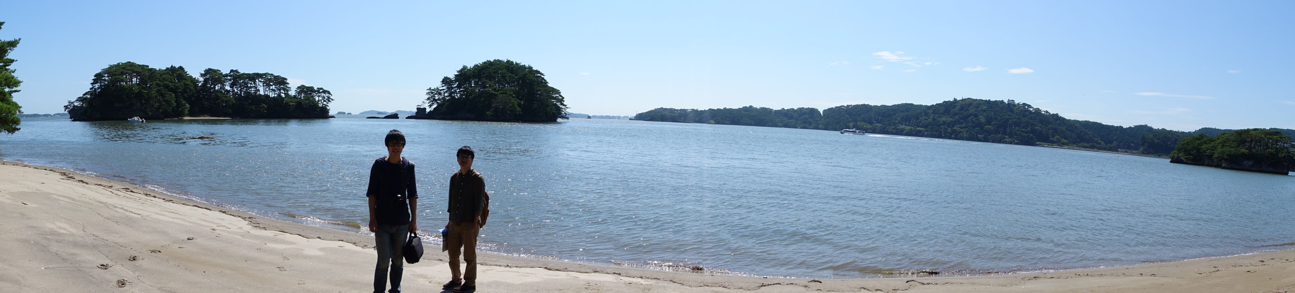
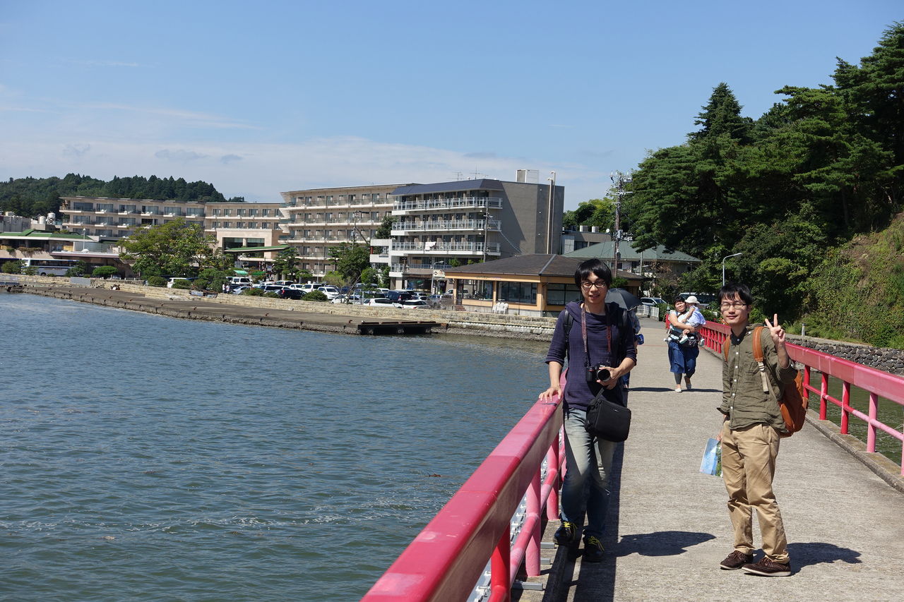
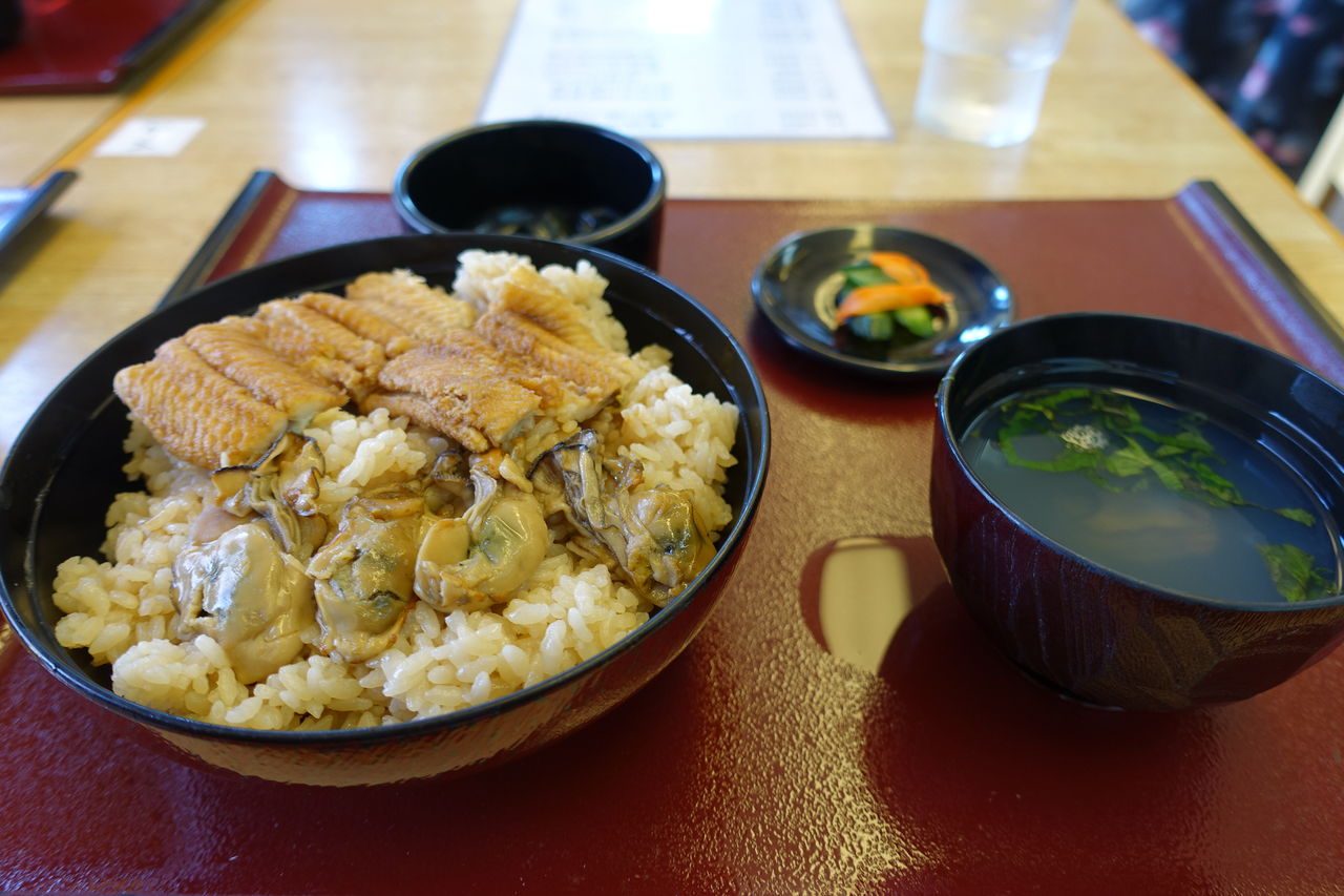
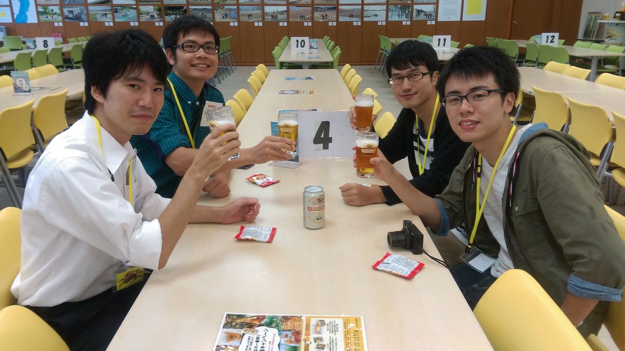
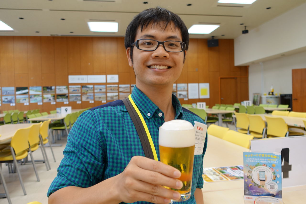
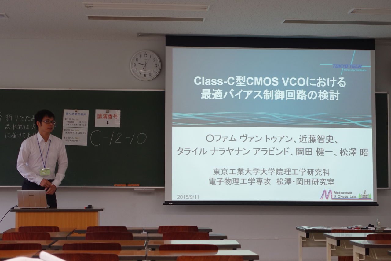
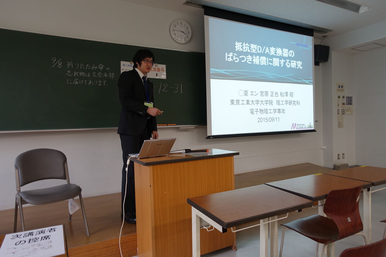
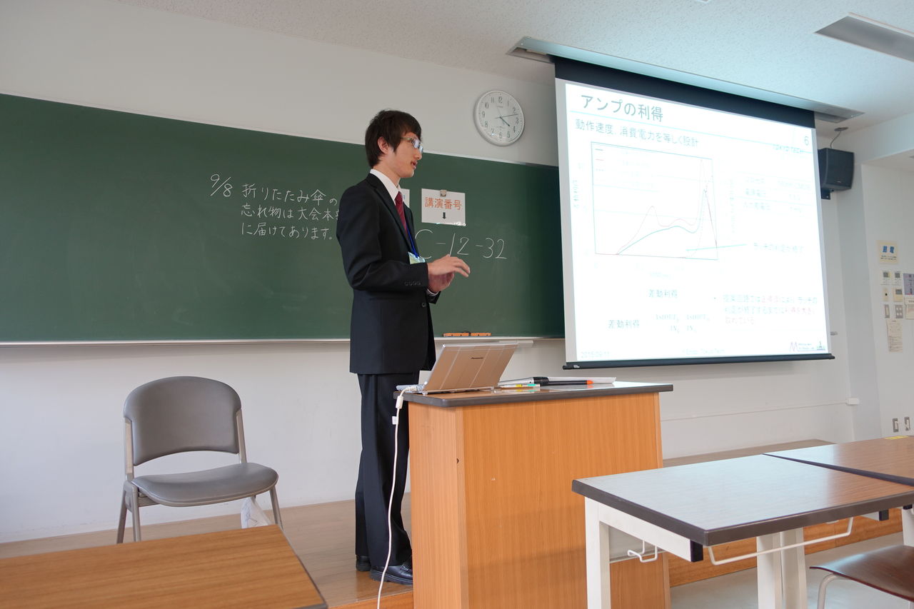
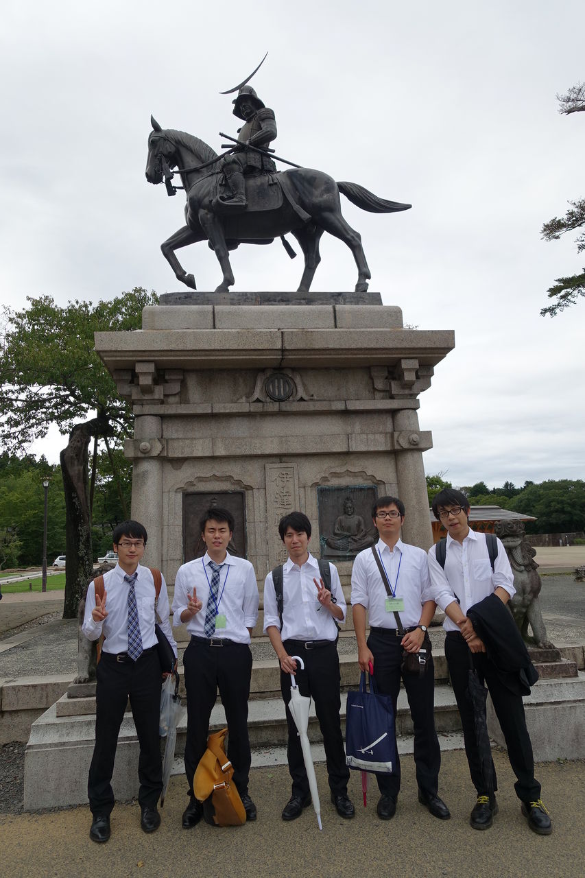
電子情報通信学会 ソサイエティ大会 @東北大
通信学会@東北大に参加してきました!
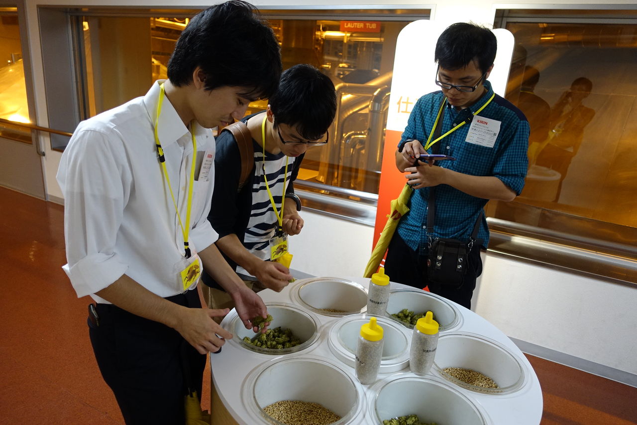
キリンの工場でビールの作り方を勉強したりしました。
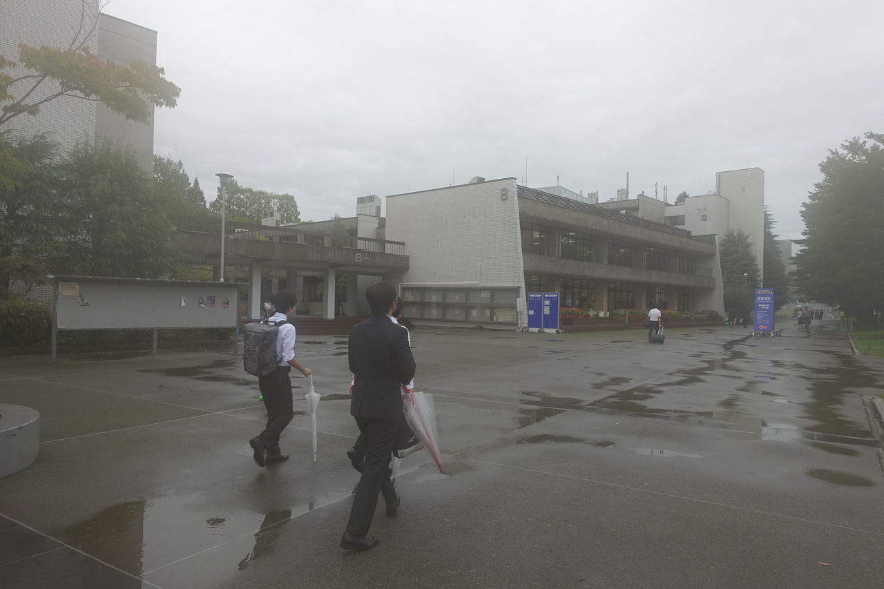
発表日は豪雨で電車・バスが止まっており、駅から40分ほど歩く羽目に…。
以上です!
For Foreign Students
International Graduate Program http://www.titech.ac.jp/english/globalization/stories/international_graduate_program.html
See also this.

OB会3次会
published on
VDECデザイナーズフォーラム2015
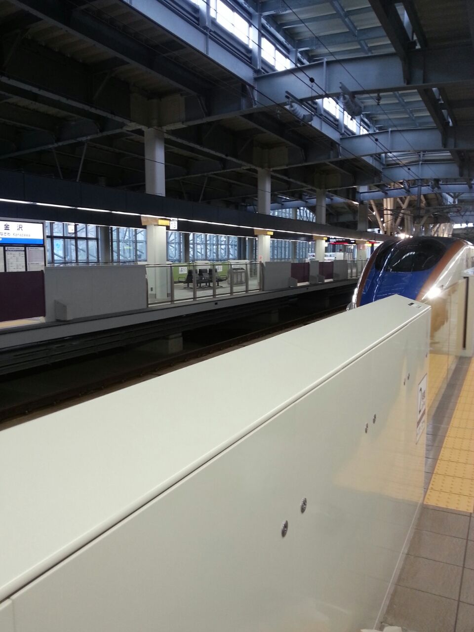
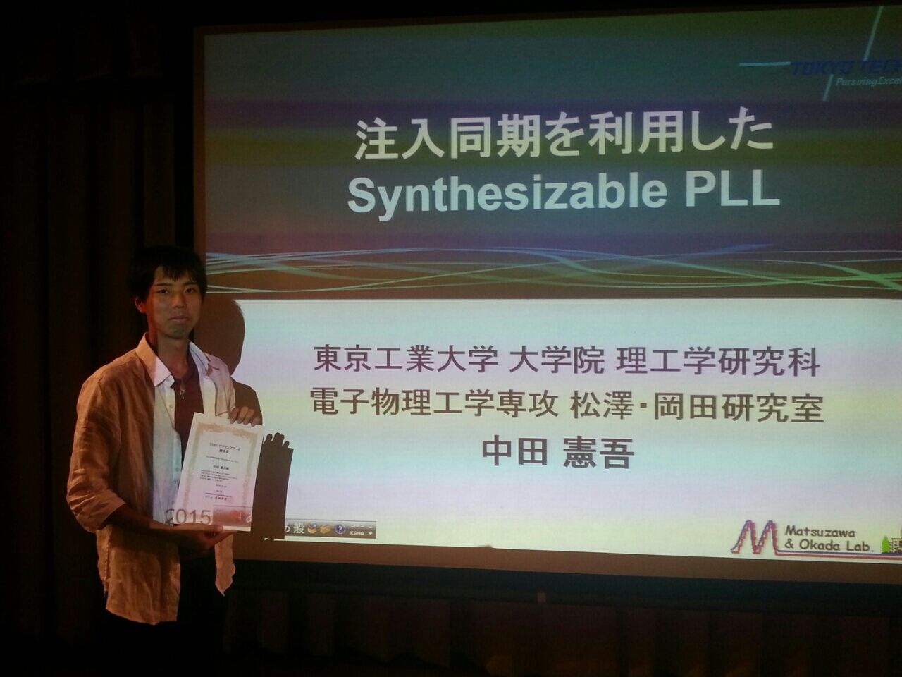
M2の中田です。
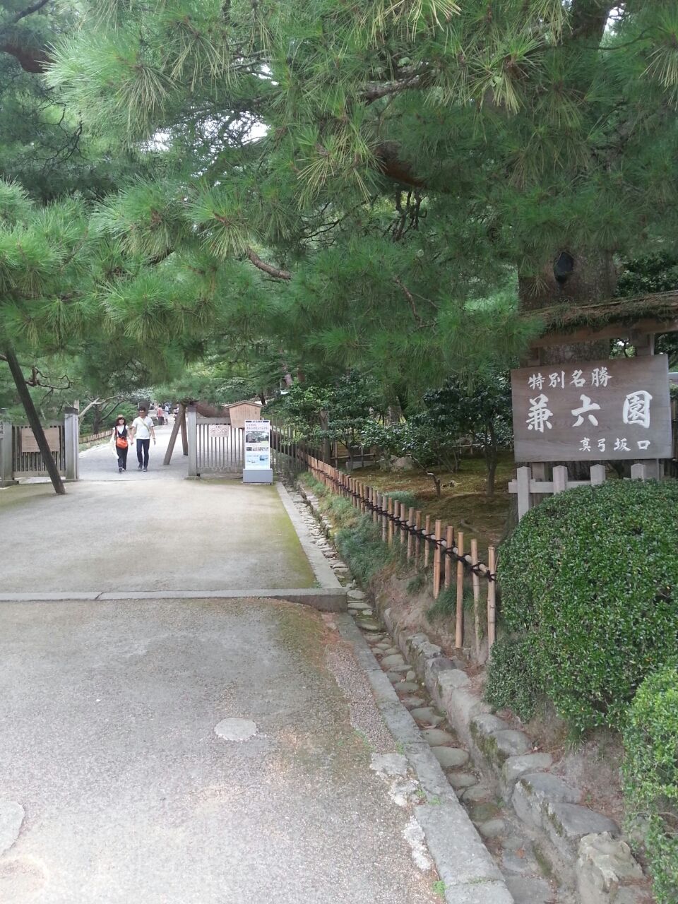
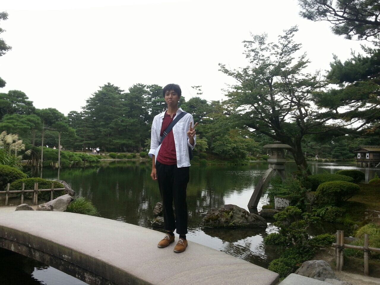
今年開通した北陸新幹線に乗って、石川県加賀市で行われたVDECデザイナーズフォーラム2015に参加してきました。
そしてデザインアワード部門にて発表し、優秀賞をいただくことができました。
OB会
一次会飛ばして二次会からです
これだけでいろいろわかると思います

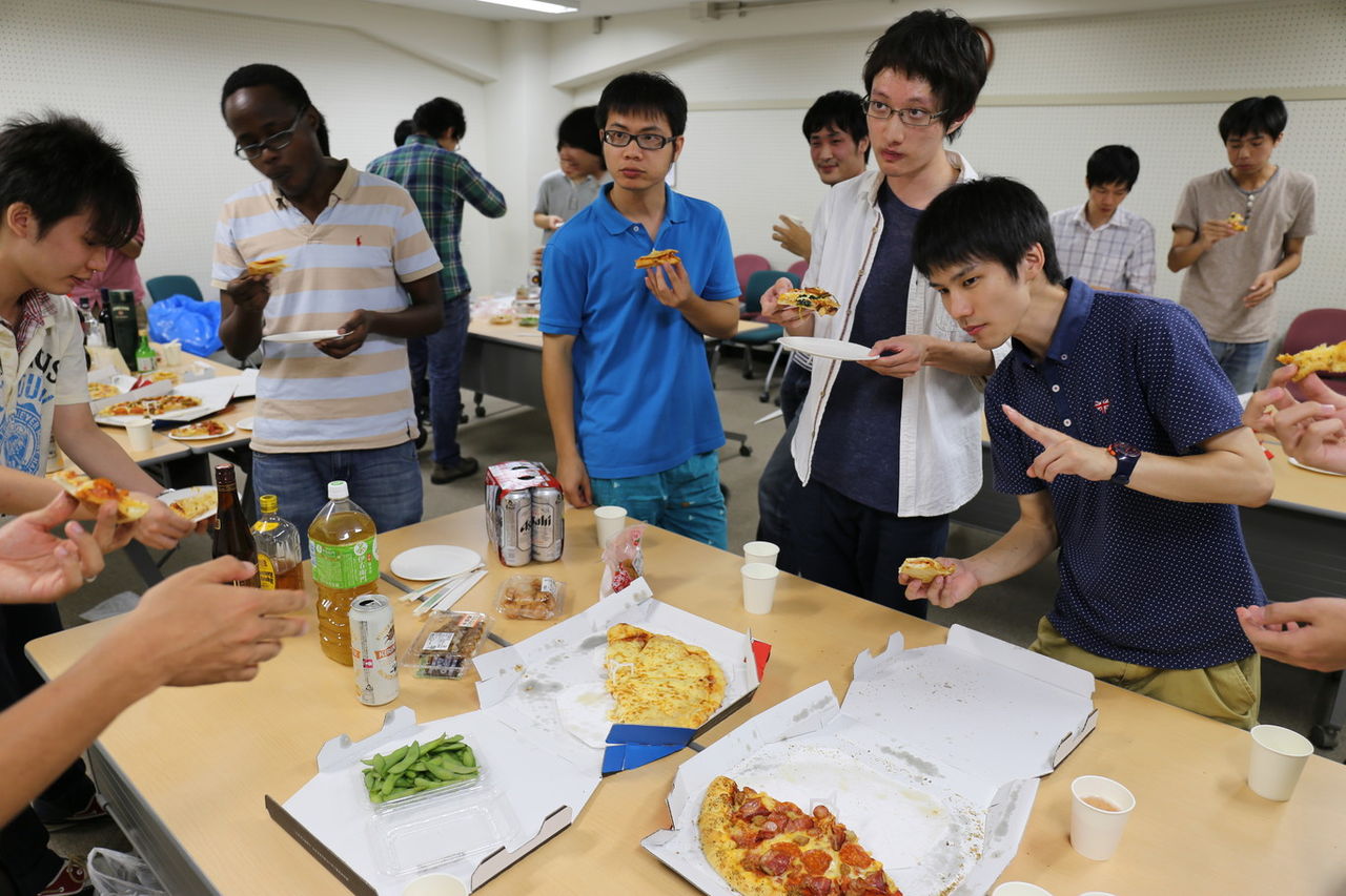
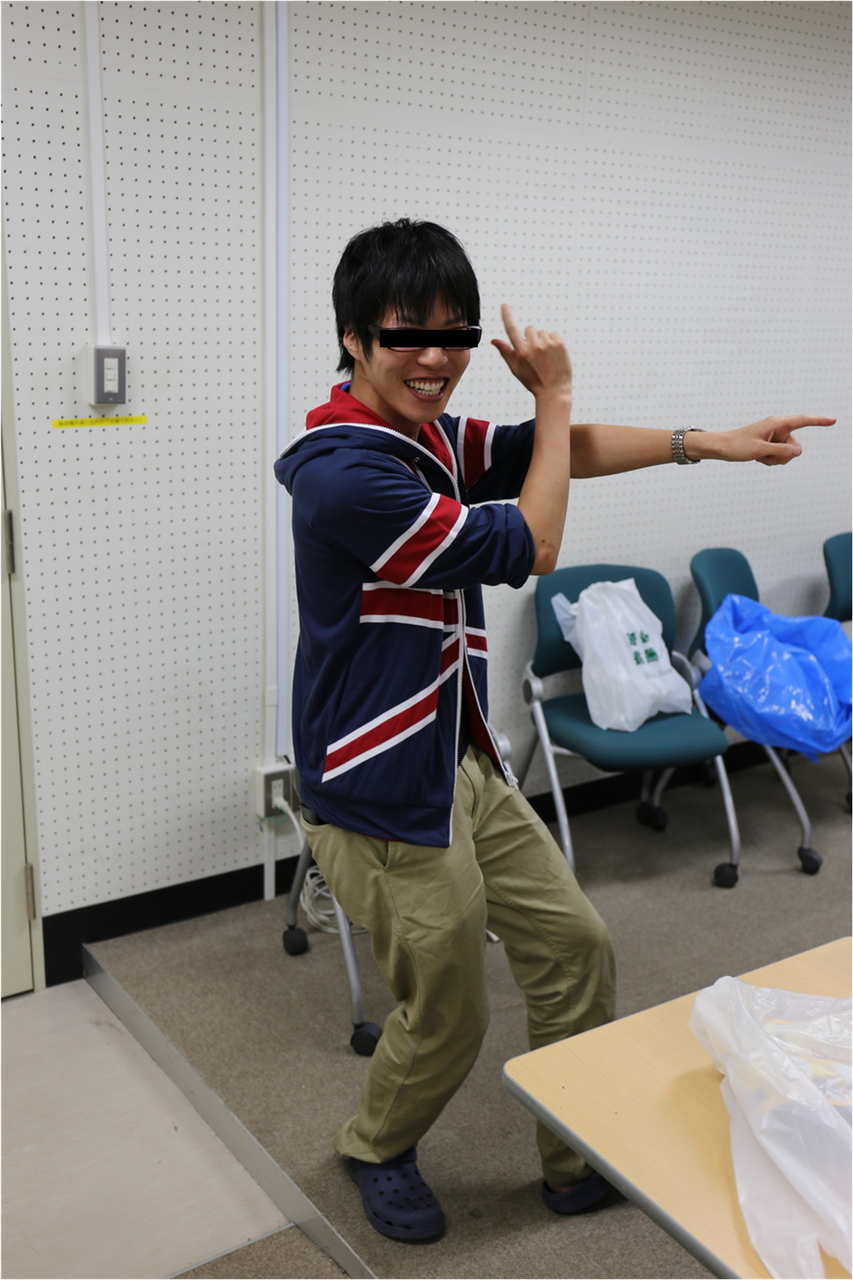
B4院試お疲れピザパーティ
published on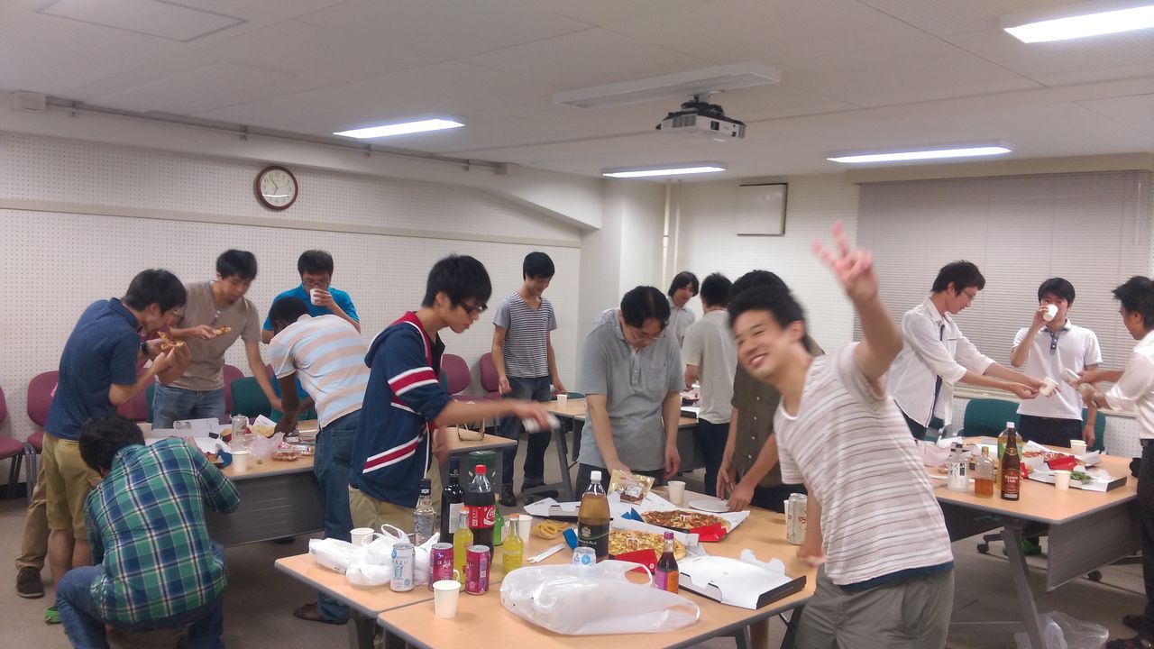
For Foreign Students
Tokyo Institute of TechnologyInternational Graduate Program (A) (IGP-A)
Admission Date: September 23, 2016Types of Programs: Integrated Doctoral Education Program (Master+Doctor, 5 years)Application Period: August 3, 2015 - November 30, 2015http://www.titech.ac.jp/english/graduate_school/international/graduate_program_a/index.htmlhttp://www.titech.ac.jp/english/graduate_school/international/graduate_program_a/program1.htmlhttp://www.titech.ac.jp/english/graduate_school/international/graduate_program_a/pdf/list1_2016a.pdf
Sustainable Engineering Program -> Information and Communication Technology Course -> Dept. of Electrical and Electronic Engineering
A limited number of students with outstanding academic records are eligible to apply for a scholarship from Japan’s Ministry of Education, Culture, Sports, Science and Technology (“MEXT”) with a recommendation from Tokyo Tech.Preliminary application
A preliminary application is required. Please see here.===================== FAQ =====================* Q1. Is it possible to finish only master course in 2 years?
* A1. No. This program is only for the 5-year master and doctor integrated course. The total period depends on the research progress, so it sometimes becomes shorter or longer.* Q2. Is Japanese language skill required?
* A2. No. You have no need to speak Japanese for your study. However, I would recommend to study Japanese for enjoying you daliy life in Japan.* Q3. English scope?
* A3. Your English score such as TOEFL-iBT, TOEFL-PBT, TOEIC, IELTS is required, which has to be issued within 2 years as of admission (December). There is no bottom line in the English score for your admission, but you have to be qualified for your graduation. See this for details.* Q4. Entrance examination?
* A4. Mathematics, Electrical Circuits, Electromagnetism. See this (past exam, not for this time).===================== research projects =====================
publication list
-- Millimeter-wave transceiver
1 (ppt), 2
- Digital Frequency Synthesizer
1 (ppt), 2 (ppt)
- Ultra-low-power wireless transceiver for IoT Started from this year.
- Chip-Scale Atomic ClockStarted from this year.

オープンキャンパス
published on
自由が丘
published on